High Carrier Mobility in Cubic Boron Arsenide Advances Semiconductor Materials Research
Physics World has included the groundbreaking work of University of Houston researchers on its list of Top 10 breakthroughs of 2022 for demonstrating cubic boron arsenide as “one of best semiconductors known to science.”
Two independent teams, one led by Zhifeng Ren at UH and Gang Chen at the Massachusetts Institute of Technology, and the other led by UH’s Ren and Jiming Bao along with Xinfeng Liu of the National Center for Nanoscience and Technology in China, experimentally validated the cubic boron arsenide crystal’s high carrier mobility for both electrons and holes – the two ways in which a charge is carried in a semiconducting material.
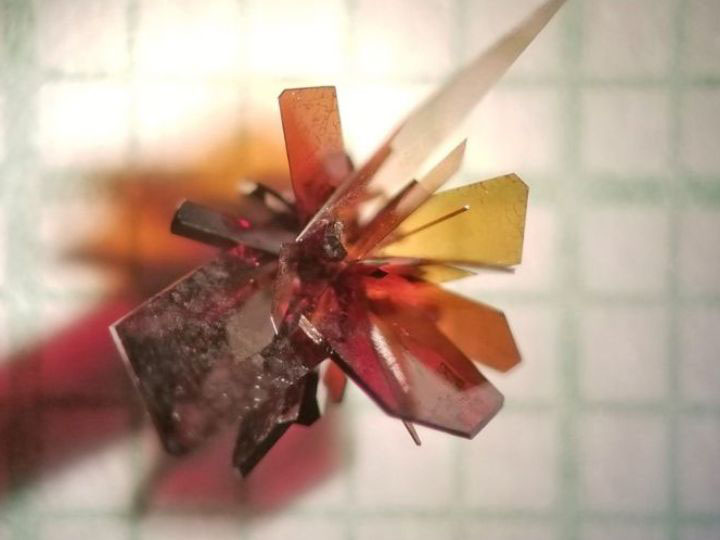
The crystal – grown from boron and arsenic since 2015 in Ren’s lab, two relatively common mineral elements – demonstrated far higher thermal conductivity than traditional semiconductors in 2018.
This is important because semiconductors require that current be carried both through electrons and holes, but most known materials offer high mobility for only one type of carrier. The overall efficiency of the semiconductor is determined by the lower value. This makes the cubic boron arsenide crystals very efficient and the potential for practical applications that much closer thanks to this leading research.
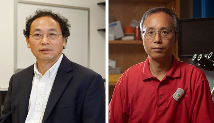
Ren, director of the Texas Center for Superconductivity at UH, said the work has important implications for a range of electronic and optical applications, like the advances that followed the advent of silicon wafers, which are widely used in all kinds of electronics.
“The potential of this material is tremendous,” said Ren, who is also M.D. Anderson Chair Professor of physics. While work to consistently produce larger crystals with uniform properties is ongoing, the result could have an even bigger impact on the field than the silicon wafer, he said.
How the Research Was Done
The first step was to grow better crystals in Ren’s lab. Then, according to Bao, professor of electrical engineering and a principal investigator with the Texas Center for Superconductivity, researchers used laser pulses to excite carriers in the sample to monitor their diffusion and, in the process, discovered a key difference between the cubic boron arsenide crystal and most semiconducting materials. In silicon, for example, he said electrons move about four times more quickly than holes.
“In this case, both the holes and electrons move more quickly,” he said adding that both electrons and holes exhibited unusually high mobility, improving the material’s overall performance.
Bao attributed the highest measurements to “hot electrons,” which maintained heat, or energy generated by the laser pulse, longer than they do in most other materials. The same was true of holes in the material, Bao said.
The structure of the cubic boron arsenide crystal makes it more difficult for the charge carriers to cool, meaning they maintain the heat – and the resulting high mobility – for longer. The measurements were performed using different methods in labs at UH and MIT.
Read about the Physics World’s Top 10 Breakthroughs of 2022.
- Rashda Khan, University Media Relations