Computer Workstations
- 1TB Ram
- Two Intel Xenon Gold 2.2 GHz, 24 cores
- Windows 11 Pro
- 12 TB Hard Drive
- Two 55 inch 8K monitors
- Digital Micrograph software
- Velox software
- Aviso software for image processing including 3D reconstruction
Available Spring 2025
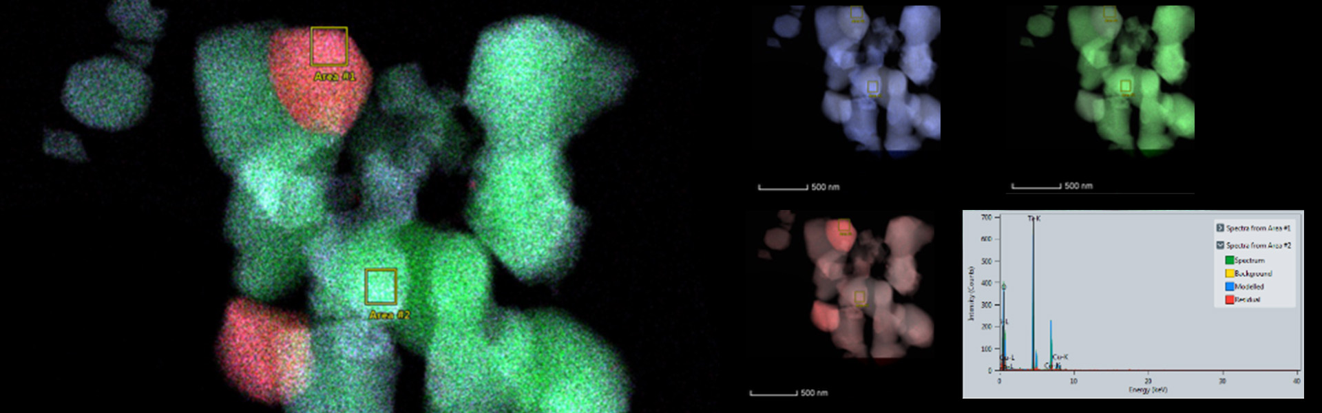
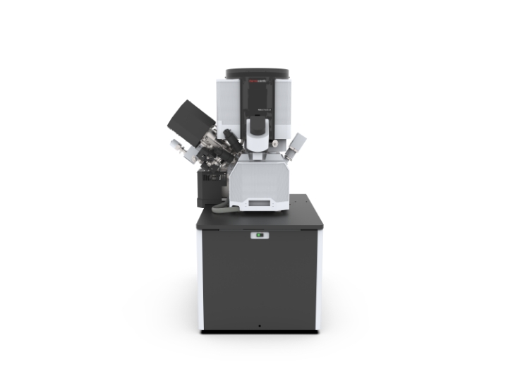
JEM-ARM300F2 (GRAND ARM™2 Atomic Resolution Analytical Microscope) equipped with a Cold Field Emission electron Gun (Cold-FEG) which provides a smaller energy spread from the electron source for 300 kV and 60 kV. At 300 kV, the STEM image resolution with the standard probe conditions of a Cs-corrected can reach 53 pm. The system is equipped with energy dispersive X-ray spectroscopy (EDS) with FHP2 objective lens pole piece, it can provide higher X-ray detection efficiency (1.4sr) with sub-angstrom resolution in EDS elemental maps. Next-generation Gatan imaging filter that enables electron energy loss spectroscopy (EELS) and energy-filtered transmission electron microscopy (EFTEM), The energy resolution of the Electron Energy-Loss Spectroscopy (EELS) is up to 0.3 eV. The OBF (Optimum Bright Field) STEM has an advantage for low dose imaging, such as beam sensitive materials including Metal Organic Frameworks (MOFs) and Zeolites require a reduced electron dose while maintaining clear atomic contrasts for the framework of light elements.


Guanhui (Gigi) Gao Holland, Ph.D.
Research Manager of Electron Microscopy Core
(713) 743- 6458
Email: ggao7@central.uh.edu
Google Scholar
Room 112, 116, Durga D. and Sushila Agrawal Engineering Research
4218 M. L. King Blvd,
Houston, TX 77204