High Carrier Mobility in Cubic Boron Arsenide Offers Promise for Next-Gen Electronics
Researchers have for the first time experimentally discovered that a cubic boron arsenide crystal offers high carrier mobility for both electrons and holes – the two ways in which a charge is carried in a semiconducting material – suggesting a major advance for next-generation electronics.
While earlier predictions had theorized that the crystal could exhibit simultaneously high electron and hole mobility, one of two papers published July 22 in the journal Science shows that researchers were able to experimentally validate the high carrier mobility at room temperature, expanding its potential use in commercial applications. Researchers from across the United States, including the University of Houston, the Massachusetts Institute of Technology, the University of Texas at Austin and Boston College, were involved in the work.
An accompanying paper in the July 22 edition of Science describes the use of transient reflectivity microscopy to measure the crystal, demonstrating the high mobility and in some cases, when a higher-energy laser beam was used, exceeding previous predictions. That work was done by researchers from UH and from the National Center for Nanoscience and Technology in Beijing, along with several other institutions in China.
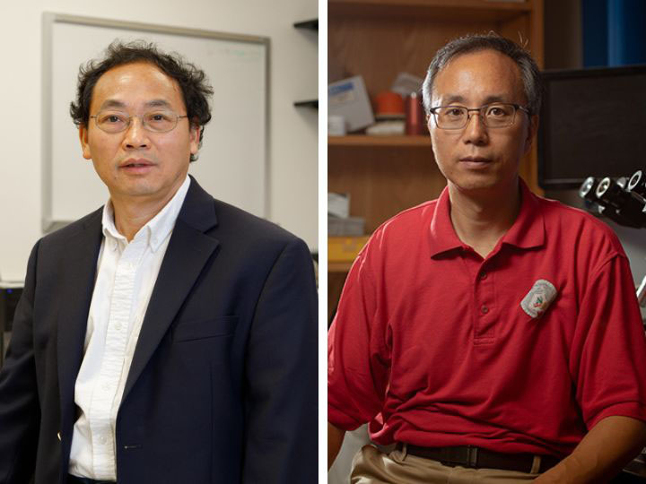
Zhifeng Ren, director of the Texas Center for Superconductivity at UH and a corresponding author on both papers, said the work has important implications for a range of electronic and optical applications, similar to the advances that followed the advent of silicon wafers, which are widely used in all kinds of electronics.
Some semiconductor applications require a material with both high thermal conductivity – which measures how effectively a material conducts heat – and high electron and hole mobility. Earlier research had demonstrated cubic boron arsenide has high thermal conductivity, making the high ambipolar mobility a crucial advance.
“The potential of this material is tremendous,” said Ren, who is also M.D. Anderson Chair Professor of physics at UH’s College of Natural Sciences and Mathematics. While work to consistently produce larger crystals with uniform properties is ongoing, the result could have an even bigger impact on the field than the silicon wafer, he said.
That’s because semiconductors require that current be carried both through electrons and holes, but most known materials offer high mobility only for one type of carrier. The overall efficiency of the semiconductor is determined by the lower value.
“If both are high, the device will be more efficient,” Ren said. “That’s what makes this material unique.”
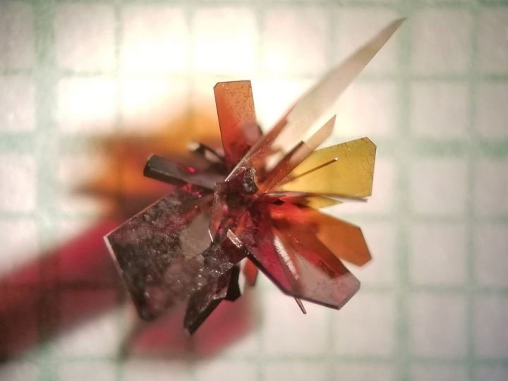
Ren was among a group of researchers who reported in Science in 2018 that the crystal – grown from boron and arsenic, two relatively common mineral elements – demonstrated far higher thermal conductivity than traditional semiconductors. This work builds on that, using crystals grown in Ren’s lab to demonstrate that theoretical predictions about the substance’s high mobility can be shown experimentally.
Carrier mobility is measured in the unit of cm2V-1s-1; the researchers reported mobility of 1,600 cm2V-1s-1. That portion of the work was led by Gang Chen, Carl Richard Soderberg Professor of Power Engineering at MIT and co-corresponding author of the paper, using an optical transient grating method to measure both electrical mobility and thermal conductivity.
In the second paper, researchers led by Ren and Jiming Bao of UH and Xinfeng Liu at the National Center for Nanoscience and Technology in Beijing, reported a range from about 1,500 cm2V-1s-1 to as high as 3,000 cm2V-1s-1.
Measuring carrier mobility was complicated by the fact that the crystal wasn’t large and uniform, meaning traditional measurement methods such as the Hall effect couldn’t accurately determine its properties. The researchers said that ionized impurities weakened the material’s performance by strongly scattering the charge carriers, although other impurities – described in the paper as “neutral impurities” – had less of an impact.
“The sample was not uniform, but you can see the potential locally,” Ren said. “If you had a crystal free of defects, mobility could be potentially much higher than predicted. We are in continuous research to figure that out.”
The measurements were performed using different methods in labs at UH and MIT.
In the second paper, researchers from UH and six Chinese universities and institutions describe the use of transient reflectivity microscopy to measure the electron and hole mobility.
Bao, professor of electrical engineering at UH and a principal investigator with the Texas Center for Superconductivity, said researchers used laser pulses to excite carriers in the sample to monitor their diffusion and, in the process, discovered a key difference between the cubic boron arsenide crystal and most semiconducting materials. In silicon, for example, he said electrons move about four times more quickly than holes.
“In this case, the holes move more quickly than electrons,” he said. But both electrons and holes exhibited unusually high mobility, improving the material’s overall performance.
Bao attributed the highest measurements, which detected mobility far higher than 1,600 cm2V-1s-1, to “hot electrons,” which maintained heat, or energy, generated by the laser pulse longer than they do in most other materials. The same was true of holes in the material, Bao said.
The structure of the cubic boron arsenide crystal makes it more difficult for the charge carriers to cool, meaning they maintain the heat – and the resulting high mobility – for longer. The researchers reported mobility similar to the predicted levels and those found by Chen’s lab but noted that additional experiments revealed a mobility of more than 3,000 cm2V-1s-1, which they attributed to the hot electrons.
The findings depended in part on measuring a section of the crystal with few or no impurities, Bao said. “The sample was not uniform, and we found the highest mobility at spots with the fewest impurities.”
In addition to Ren and Chen, researchers involved in the work to demonstrate high mobility include Geethal Amila Gamage and Fei Tian of UH; Jungwoo Shin, Zhiwei Ding, Ke Chen, Xin Qian, Jiawei Zhou, Aaron Schmidt, Thanh Nguyen, Fei Han and Mingda Li of MIT; Hwijong Lee, Li Shi and Jianshi Zhou of the University of Texas at Austin; and David Broido of Boston College.
Bao’s collaborators, in addition to Ren and Liu, include Shuai Yue, Fei Tian, Mohammadjavad Mohebinia and Tian Tong, all with UH; Xinyu Sui and Xianxin Wu, with the National Center for Nanoscience and Technology and the University of Chinese Academy of Sciences; Zhiming Wang with the University of Electronic Science and Technology of China; Bo Wu of South China Normal University; and Qing Zhang of Peking University.
- Jeannie Kever for Texas Center for Superconductivity at UH